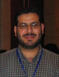
Yaser M. Haddara
Ph.D. (Electrical Engineering), Stanford University, 1997
M.Sc. (Electrical Engineering), Stanford University, 1993
B.Eng. (Electrical Engineering), Memorial University of Newfoundland,
1991
Department of Electrical and Computer Engineering
ITB-A223
T: 905.525.9140 x24968
F: 905.521.2922
E: yaser@mcmaster.ca
Research Interests
- Semiconductor
process modeling; Silicon Germanium process and device modeling;
Silicon Carbide process and device modeling; Diffusion, oxidation, and
point defects in semiconductors
- Engineering education; problem based learning; online and blended learning; active learning spaces
Teaching Interests
Microelectronic
devices and circuits; Introduction to electrical engineering;
Processing and characterization of semiconductor materials and devices;
Mathematics of diffusion; Semiconductor device physics and modeling;
Electronic, optical, and magnetic properties of materials; Polymer
semiconductors
Current Research Projects
- Si-Ge interdifusion and point defects in SiGe
- SiGe Oxidation
- Cobalt Germanidation
- Implant damage and diffusion in SiC
Recent Publications
- Yaser
M. Haddara, Peter
Ashburn, and Darren Bagnall, "Silicon-Germanium: Properties, Growth, and Applications,“
in Springer Handbook of Electronic and Photonic Materials, Safa Kasap
and Peter Capper (eds.), 2nd ed., Springer (2016), In press.
- Mohammad
Hasanuzzaman,
Yaser M. Haddara, and Andrew P. Knights, “Role of a Si0.95Ge0.05
epilayer cap on boron diffusion in silicon under inert and dry oxidizing
ambient annealing,” accepted for publication, Mat. Sci. Semicon. Proc.,
2016.
- Yiheng Qin, Matiar M.R.
Howlader, M. Jamal Deen, Yaser M. Haddara, P. Ravi Selvaganapathy, “Polymer
integration for packaging of implantable sensors,” Sensors and Actuators, B:
Chemical, v. 202, pp. 758-778, 31 October, 2014.
- Ahmed Fakhr and Yaser M.
Haddara, “Modeling of InGaP nanowires morphology and composition on molecular
beam epitaxy growth conditions,” J. Appl. Phys., v. 116, p. 024314 (10
pp.), 14 July 2014.
- Ahmed
Fakhr,
Yaser M. Haddara, and Ray R. LaPierre, “Modeling Growth,
Morphology, and Composition of Ternary III-V Nanowires,” IEEE – 2013 Saudi
International Electronics, Communications, and Photonics Conference, Riyadh,
Saudi Arabia, April 27-30, 2013.
- M.
Hasanuzzaman,
Y.M. Haddara, and A.P. Knights, “A mathematical model for void evolution in
silicon by helium implantation and subsequent annealing process,” J. Appl.
Phys., 112, 064302 (10 pp.), 15 Sept. 2012.

