
|
HADI |
Hardware Accelerated Design and Integration Research Laboratory 
|
Research
Ameer Abdelhadi
People
Vacancies
Publications
Teaching
Open Source
Contact
Looking ahead, our research will emphasize hardware-efficient domain-specific acceleration, particularly for machine learning and neuroscience applications. This involves leveraging hybrid platforms such as FPGAs and ASICs to serve as spatially parallel accelerators. Our goal is to create hardware-efficient, domain-specific architectures that balance programmability, configurability, cost-effectiveness, power efficiency, and performance. Another exciting frontier involves designing efficient hardware architectures for brain data analysis and decoding.
Beyond these primary pursuits, our broader research interests include:
- Advancements in hardware-efficient deep learning and its applications,
- Innovations in neurotechnology and brain-computer interfaces,
- Massively parallel reconfigurable system architectures,
- CAD algorithm development for VLSI physical design automation, and
- Asynchronous circuits and clock domain crossing management.
| Sponsors: |
|
Neurotechnology
See our MICRO 2021 paper for more details.
[Paper: PDF, HTML5, DOI] [Slides: PDF]
NOEMA 1.0 has been fabrication! See our Hot Chips 2022 paper form more details.
[Paper: PDF, DOI] [Slides: PDF] [Chip (fabricated): NEOMA 1.0]

Hardware-Efficient Deep Learning
"People who are really serious about software should make their own hardware." —Alan Kay, Creative Think seminar, 1982.
Since the beginning of the current century, great achievements in machine learning have been possible due to significant advancements in big data processing. In particular, deep learning—bio-inspired artificial neural networks—has become the default standard for a variety of complex tasks, such as recognition, classification, and natural language processing. Adapting to ever-increasing workloads, deep learning algorithms have become extremely compute- and memory-intensive, making them infeasible for deployment on compact, embedded platforms with power and cost budget limitation. Moreover, the majority of deep learning applications require real-time, low-latency processing. Due to their complexity, deep learning applications require massive computing systems, hence they are rarely found in consumers’ devices. Recently, Graphics Processing Units (GPUs)—highly-parallel processing arrays—are successfully exploited to accelerate deep learning applications. However, their integration into embedded, mobile, and robotic systems—in which most machine learning algorithms are applicable—is latency, memory, power, and cost prohibitive. Alternatively, special-purpose hardware devices are leveraged by the leading technology vendors (e.g. Google's Tensor Processing Unit (TPU)) to satisfy low-latency, and real-time requirements while limiting the power envelop. Typically, these devices are designed to accommodate the majority of deep learning applications, which adversely reduces their efficiency. With the demise of Moore's law, a new era has begun; silicon technology scaling has become saturated. Thus, technology scaling alone cannot provide more efficient platforms for machine learning. My research suggests algorithmic and system-level approaches for highly efficient machine learning platforms.Accelerated Approximate Nearest Neighbors Search through Hierarchical Product Quantization
A fundamental recurring task in many machine learning applications is the search for the Nearest Neighbor in high dimensional metric spaces. Towards answering queries in large scale problems, state-of-the-art methods employ Approximate Nearest Neighbors (ANN) search, a search that returns the nearest neighbor with high probability, as well as techniques that compress the dataset. Product-Quantization (PQ) based ANN search methods have demonstrated state-of-the-art performance in several problems, including classification, regression and information retrieval. PQ methods encode the dataset into a Cartesian product of multiple low-dimensional codebooks, enabling faster search and higher compression. Being intrinsically parallel, PQ-based ANN search approaches are amendable for hardware acceleration. This work proposes a novel Hierarchical PQ (HPQ) based ANN search method as well as an FPGA-tailored architecture for its implementation that outperforms current state of the art systems. As illustrated, HPQ gradually refines the search space, reducing the number of data compares and enabling a pipelined search. The mapping of the architecture on a Stratix 10 FPGA device demonstrates over x250 speedups over current state-of-the-art systems, opening the space for addressing larger datasets and/or improving the query times of current systems. The HPQ algorithm and its hardware acceleration have a tangible impact on the feasibility of Sparse Memory Augmented Neural Networks, such as the Sparse Neural Turing Machine from Google DeepMind. Sparse Memory Augmented Neural Networks rely heavily on space-splitting metric trees to perform nearest neighbors search; however, these data structures are not scalable, rendering it infeasible for practical application. The HPQ method has been published in the 2019 International Conference on Field-Programmable Technology (FPT) and has been nominated for the best paper award. [Paper: PDF]
Fine-Grained Inference Engine Utilizing Online Arithmetic
Modern Deep Neural Networks (DNNs) exhibit incredible performance on a variety of complex tasks, such as recognition, classification, and natural language processing. Adapting to ever-increasing workloads, deep learning algorithms have become extremely compute- and memory-intensive, making them infeasible for deployment on compact, embedded platforms with power and cost budget limitation. Common methods to minimize and accelerate deep learning involve pruning, quantization, and compression of the neural model. While these techniques show a dramatic model reduction, in several cases they incur an accuracy degradation. Moreover, methods involving custom hardware still suffer from large silicon footprint and high power consumption due to massive computations and external memory accesses. This work employs online Most Significant Digit (MSD) first digit-serial arithmetic to enable early termination of the computation. Using online MSDF bit-serial arithmetic for DNN inference (1) enables early termination of ineffectual computations, (2) enables mixed-precision operations, (3) allows higher frequencies without compromising latency, and (4) alleviates the infamous weights memory bottleneck. The proposed technique is efficiently implemented on FPGAs due to their concurrent fine-grained nature, and the availability of on-chip distributed SRAM blocks. Compared to other bit-serial methods, our Fine-Grained Inference Engine (FGIE) improves energy efficiency by x1.8 while having similar performance gains. The FGIE architecture has been published in the 2019 International Conference on Field-Programmable Technology (FPT). [Paper: PDF]
(bottom) An FGIE layer. Computes p neurons with s synapses each.
Massively Parallel Reconfigurable Architectures
Leveraging Massively Parallel Hardware to Bridge the Performance Gap Between FPGAs and ASICs
My long-term future research plans are to bridge the performance gap between FPGAs and ASICs.
I believe that utilizing the concurrent nature of FPGAs by providing massively parallel architectures is the key for performance-oriented systems.
However, this requires changes in the underlying reconfigurable architecture, the support of CAD tools, and proposing highly efficient parallel system to utilize these changes.
 Since they were first introduced three decades ago, field-programmable gate arrays (FPGAs) have evolved from being merely used as glue-logic to competing with custom-designed application-specific integrated circuits (ASICs).
Modern FPGAs comprise hundreds of thousands of programmable logic gates augmented with thousands of configurable digital signal processing (DSP) blocks and memory blocks, all on the same chip with flexible routing fabric.
Routing and configuration flexibility of these numerous hardware blocks grants FPGAs their inherent parallelism; hence, FPGAs are exploited for massively parallel computing and can be tailored as an accelerator for specific applications.
Since they were first introduced three decades ago, field-programmable gate arrays (FPGAs) have evolved from being merely used as glue-logic to competing with custom-designed application-specific integrated circuits (ASICs).
Modern FPGAs comprise hundreds of thousands of programmable logic gates augmented with thousands of configurable digital signal processing (DSP) blocks and memory blocks, all on the same chip with flexible routing fabric.
Routing and configuration flexibility of these numerous hardware blocks grants FPGAs their inherent parallelism; hence, FPGAs are exploited for massively parallel computing and can be tailored as an accelerator for specific applications.
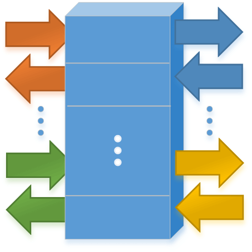
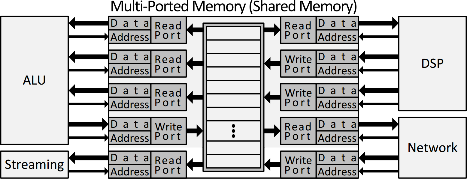
My general long-term research interests are architecture, design methodologies and computer-aided-design for parallel computing systems, particularly in the area of FPGAs and reconfigurable computing. In particular, I am interested in resolving the memory bottleneck of massively parallel reconfigurable systems by providing efficient, parallel and customizable embedded memory structures. Although concurrent multi-ported memories are important, their high implementation cost means they are used sparingly. As a result, FPGA vendors only provide standard dual-ported memories to handle the majority of usage patterns. My research provides a novel, efficient and modular approach to construct multi-ported memories out of basic dual-ported RAM blocks; this opens the door to future research of new parallel reconfigurable and customizable architectures based on these concurrent memories.
Another massively parallel memory structure that I am interested to investigate in the near future is the content-addressable memory (CAM), a hardware implementation of associative arrays. Despite their vast importance, FPGAs lack an area-efficient CAM implementation. In my research, I proposed to construct SRAM-based, efficient and modular binary CAMs. However, this is just the tip the iceberg as reconfigurable devices provide the flexibility to develop a new series of customizable application-specific associative arrays, such as ternary CAMs.
Multi-ported memories - Revisiting the memory bottleneck
 Massively parallel systems demand highly parallel memory structures to keep pace with their concurrent nature since memories are usually the bottleneck of computation performance.
The vast majority of FPGA devices provide dual-ported SRAM blocks only.
This allows RAM content in one block to be accessed concurrently by two "users" at the same time.
To allow more concurrent access, a method is required for organizing potentially thousands of RAM blocks.
In my dissertation, I propose new ways to build area-efficient, high-performance parallel memory structures in FPGAs using the regular dual-ported memory blocks found in modern FPGAs.
Massively parallel systems demand highly parallel memory structures to keep pace with their concurrent nature since memories are usually the bottleneck of computation performance.
The vast majority of FPGA devices provide dual-ported SRAM blocks only.
This allows RAM content in one block to be accessed concurrently by two "users" at the same time.
To allow more concurrent access, a method is required for organizing potentially thousands of RAM blocks.
In my dissertation, I propose new ways to build area-efficient, high-performance parallel memory structures in FPGAs using the regular dual-ported memory blocks found in modern FPGAs.
Multi-ported memories are the cornerstone of all high-performance CPU designs. They are often used in register files, but also in other shared-memory structures such as TLBs, caches and coherence tags. In particular, multi-ported RAMs are often used by wide superscalar processors, VLIW processors, multi-core processors, coarse grain reconfigurable arrays (CGRAs), and digital signal processors (DSPs). The key requirement for all of these designs is fast, concurrent, single-cycle access from multiple requesters. While there is demand for more RAM ports, the two leading multi-ported RAM techniques in FPGAs have relatively large overhead in (1) register usage or (2) total SRAM block count. In my dissertation, I produce two new design techniques that are near-optimal in resource overhead and have several practical advantages. Furthermore, I provide a mechanism to construct and optimize memory structures with time-switched ports. A RAM compiler has also been developed to automate the construction of these switched memories.
Invalidation-Live-Value-Table (I-LVT)
The I-LVT is a novel architecture and data structure to produce modular multi-ported SRAM-based memories out of dual-ported SRAM blocks only. Compared to other multi-ported approaches, the I-LVT consumes the fewest possible SRAM cells. It also provides improved overall performance. In my dissertation, I demonstrate the viability, area reduction, and performance benefits of the proposed approach and provide an open source library with a fully tested, generic and modular implementation that can be adopted in parallel computing systems.The I-LVT architecture and data structure has a tangible impact on research and industry fronts. The I-LVT architecture proposes a new SRAM-based data structure to efficiently track changes in RAM made by different users. While previous approaches use registers to implement a live-value-table, the breakthrough of my approach that it is near-optimal and purely SRAM-based, allowing it to scale to large depths. This is achieved using an invalidation-table, a novel data structure developed specially for this purpose, where a single RAM write can invalidate data in other RAM locations. The I-LVT multi-ported RAM approach has been published in the ACM/SIGDA International Symposium on Field-Programmable Gate Arrays (FPGA '14) [Paper: PDF, DOI] [Talk: PDF, PPT] [Code: GitHub] , the leading conference in FPGA technology.
Switched Ports
Switched ports, first introduced in my dissertation, are a generalization of true (bidirectional) ports, where a certain number of write ports can be dynamically switched into a different number of read ports using a common read/write control signal. While a true port is a pair of read/write ports, switched ports are best described as a set. Furthermore, a given application may have multiple sets, each set with a different read/write control. While previous work generates multi-ported RAM solutions that contain only true ports, or only simple (unidirectional) ports, my research demonstrates that using only two models is too limiting and prevents optimizations from being applied. The switched ports technique was accepted for publication at the ACM Transactions on Reconfigurable Technology and Systems (TRETS) [Paper: PDF] [Code: GitHub] in an upcoming special issue on reconfigurable components with source, a leading journal in FPGA technology.The general problem of switched ports is optimized by solving the corresponding set cover problem via ILP. This is the first time an optimization model is used to construct multi-ported RAM. Switched ports have a tangible impact on the performance of parallel computation systems (e.g. CGRAs), where the switched ports mechanism can be utilized to dramatically increase parallelism. A memory compiler that automates the construction of a multi-ported RAM with switched ports was released as an open source library. Another publication that describes this memory compiler and the optimization problem has been published in the 2016 IEEE International Symposium on Field-Programmable Custom Computing Machines (FCCM '16) [Paper: PDF, DOI] [Talk: PDF, PPT] [Code: GitHub], a leading conference in reconfigurable computing.
Associative Arrays
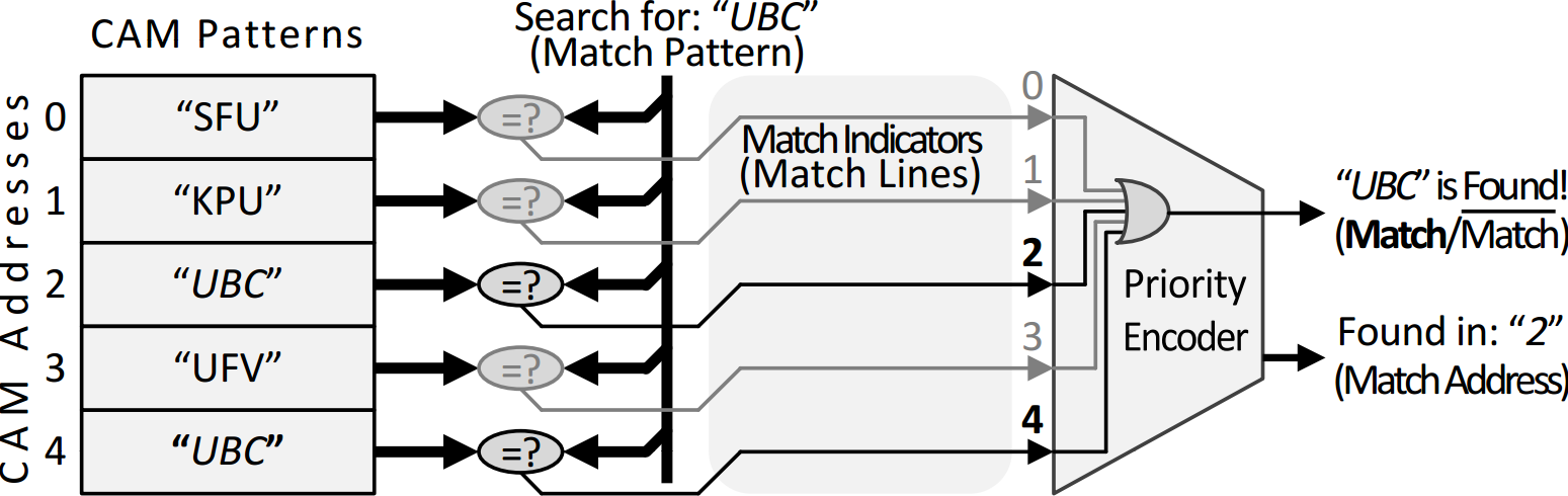
 Content-addressable memories (CAMs), the hardware implementation of associative arrays, are capable of searching the entire memory space for a specific value within a single clock cycle.
While a standard RAM returns data located in a given memory address, a CAM returns an address containing a specific given data.
To do this, it must perform a memory-wide search for a specific value, and there may be multiple addresses that all match the data.
Hence, CAMs are massively parallel search engines accessing all memory content to compare with the searched pattern simultaneously.
CAMs are also heavy power consumers due to the large memory bandwidth requirement and the concurrent compare.
CAMs are used in a variety of scientific fields requiring high-speed associative searches.
CAMs are keystones of network processors, specifically used for IP lookup engines for packet forwarding, intrusion detection, packet filtering and classification.
In addition, CAMs are used for memory management in associative caches and translation lookaside buffers (TLBs), pattern matching, data compression and databases.
Despite their importance, the high implementation cost of CAMs means they are used sparingly.
As a result, FPGA vendors do not provide any dedicated CAM circuitry or any special infrastructure to enable a construction of efficient CAMs.
Instead, designers tend to use algorithmic search heuristics causing a dramatic performance degradation.
In my dissertation, I propose two approaches to implement area-efficient binary CAMs (BCAMs).
The first approach fits deep BCAMs with narrow patterns and is capable of utilizing on-chip SRAM block as BCAMs with only 20% storage overhead.
This approach is more area-efficient even than custom-made BCAMs where the footprint of each CAM cell occupies the area of two SRAM cells.
The second approach is suitable for wide patterns and is capable of generating 9 times wider BCAMs compared to other approaches.
Content-addressable memories (CAMs), the hardware implementation of associative arrays, are capable of searching the entire memory space for a specific value within a single clock cycle.
While a standard RAM returns data located in a given memory address, a CAM returns an address containing a specific given data.
To do this, it must perform a memory-wide search for a specific value, and there may be multiple addresses that all match the data.
Hence, CAMs are massively parallel search engines accessing all memory content to compare with the searched pattern simultaneously.
CAMs are also heavy power consumers due to the large memory bandwidth requirement and the concurrent compare.
CAMs are used in a variety of scientific fields requiring high-speed associative searches.
CAMs are keystones of network processors, specifically used for IP lookup engines for packet forwarding, intrusion detection, packet filtering and classification.
In addition, CAMs are used for memory management in associative caches and translation lookaside buffers (TLBs), pattern matching, data compression and databases.
Despite their importance, the high implementation cost of CAMs means they are used sparingly.
As a result, FPGA vendors do not provide any dedicated CAM circuitry or any special infrastructure to enable a construction of efficient CAMs.
Instead, designers tend to use algorithmic search heuristics causing a dramatic performance degradation.
In my dissertation, I propose two approaches to implement area-efficient binary CAMs (BCAMs).
The first approach fits deep BCAMs with narrow patterns and is capable of utilizing on-chip SRAM block as BCAMs with only 20% storage overhead.
This approach is more area-efficient even than custom-made BCAMs where the footprint of each CAM cell occupies the area of two SRAM cells.
The second approach is suitable for wide patterns and is capable of generating 9 times wider BCAMs compared to other approaches.
Correction and Recovery of Timing Errors in Tightly Coupled CGRAs and Processor Arrays
Overclocking a CPU is a common practice among home-built PC enthusiasts where the CPU is operated at a higher frequency than its speed rating. This practice is unsafe because timing errors cannot be detected by modern CPUs and they can be practically undetectable by the end user. Using a timing speculation technique such as Razor, it is possible to detect timing errors in CPUs. To date, Razor has been shown to correct only unidirectional, feed-forward processor pipelines. Our approach safely overclocks 2D arrays by extending Razor correction to cover bidirectional communication in a tightly coupled or lockstep fashion. To recover from an error, stall wavefronts are produced which propagate across the device. Multiple errors may arise in close proximity in time and space; if the corresponding stall wavefronts collide, they merge to produce a single unified wavefront, allowing recovery from multiple errors with one stall cycle. We demonstrate the correctness and viability of our approach by constructing a proof-of-concept prototype which runs on a traditional Altera FPGA. Our approach can be applied to custom computing arrays, systolic arrays, CGRAs, and also time-multiplexed FPGAs such as those produced by Tabula. As a result, these devices can be overclocked and safely tolerate dynamic, data-dependent timing errors. Alternatively, instead of overclocking, this same technique can be used to 'undervolt' the power supply and save energy. Our method of correction and recovery of timing errors has been published in the 2013 IEEE International Symposium on Field-Programmable Custom Computing Machines (FCCM '13) [Paper: PDF, DOI] [Talk: PDF, PPT] [Code: GitHub].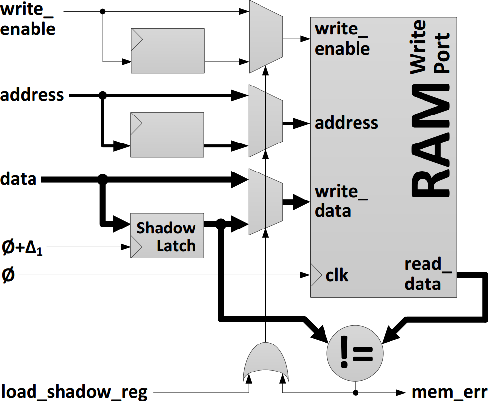
CAD Algorithms for VLSI Physical Design Automation
Synthesis of Clock Distribution Networks
Clock skew variations adversely affect timing margins, limiting performance, reducing yield, and may also lead to functional faults. Non-tree clock distribution networks, such as meshes and crosslinks, are employed to reduce skew and also to mitigate skew variations. These networks, however, increase the dissipated power while consuming significant metal resources. Several methods have been proposed to trade off power and wires to reduce skew.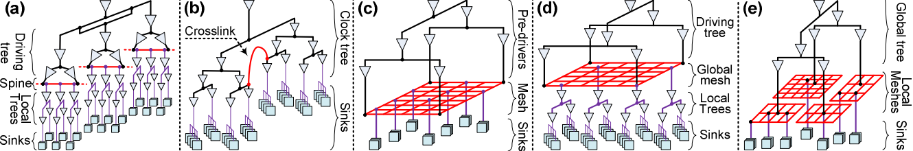
Timing-Driven Variation-Aware Nonuniform Clock Mesh Synthesis
An efficient algorithm is presented to reduce skew variations rather than skew, and prioritize the algorithm for critical timing paths, since these paths are more sensitive to skew variations. The algorithm has been implemented for a standard 65 nm cell library using standard EDA tools, and has been tested on several benchmark circuits. As compared to other methods, experimental results show a 37% average reduction in metal consumption and 39% average reduction in power dissipation, while insignificantly increasing the maximum skew. The nonuniform clock mesh synthesis algorithms have been published in the ACM/IEEE Great Lakes Symposium on VLSI (GLSVLSI '10) [Paper: PDF, DOI] [Talk: PDF, PPT] [Code: GitHub].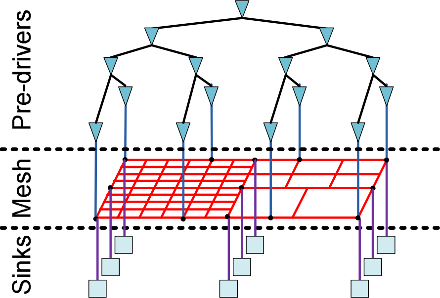
Synthesis of hybrid mesh/tree clock distribution networks
With a combination of nonuniform meshes and unbuffered trees (UBT), a variation-tolerant hybrid clock distribution network is produced. Clock skew variations are selectively reduced based on circuit timing information generated by static timing analysis (STA). The skew variation reduction procedure is prioritized for critical timing paths, since these paths are more sensitive to skew variations. A framework for skew variation management is proposed. The algorithm has been implemented in a standard 65 nm cell library using standard EDA tools, and tested on several benchmark circuits. As compared to other nonuniform mesh construction methods that do not support managed skew tolerance, experimental results exhibit a 41% average reduction in metal area and a 43% average reduction in power dissipation. As compared to other methods that employ skew tolerance management techniques but do not use a hybrid clock topology, an 8% average reduction in metal area and a 9% average reduction in power dissipation are achieved. The hybrid mesh/tree clock distribution networks synthesis approach has been published in INTEGRATION, the VLSI journal (2013) [Paper: PDF, DOI] [Code: GitHub].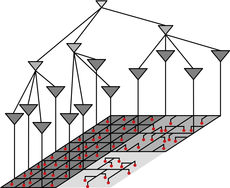
Asynchronous Circuits
A Standard-Cell Mixed-Timing Modular Synchronizing FIFO
Large system-on-chip designs typically consist of multiple timing domains motivating the use of a network-on-chip. Transferring data between these domains requires synchronization. Designers often use FIFOs because they provide a simple interface that decouples the sender and receiver actions and maximizes throughput. For network-on-chip applications, designers need synchronization FIFOs that can be constructed from components in a standard cell library and that can be configured to match the requirements of the particular design.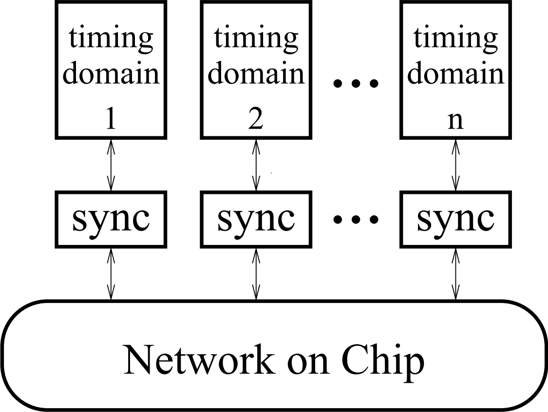
- interface protocols: clocked or clockless asP*,
- synchronization latency for resolving metastability,
- FIFO capacity, and
- storage structure: SRAM or latches.
The FIFO provides high-throughput; simulation results from extracted layout using the TSMC 90nm process show that all but one of our FIFO implementations operate at over 1Gtransfers/sec. The configurable synchronization latency supports latencies as small as half a clock period for designs operating at relatively low frequencies and more synchronization cycles for higher frequency operation. We use a standard CAD flow to synthesize and generate layout for several different synchronous and asynchronous FIFOs. Our designs can be implemented using exclusively cells available in a typical, standard cell library. Furthermore, our design is compatible with a standard ASIC design flow including static timing analysis and timing driven place-and-route; because no special CAD tools are required, our design can easily be used by mainstream designers within a standard design flow. We believe that no previous design offers the flexibility, performance and support for design within an ASIC flow that our FIFOs provide.
Our cell-based and modular mixed-timing synchronizing FIFOs have been presented in the IEEE/ACM 2012 International Conference on Computer-Aided Design (ICCAD '12): Workshop on CAD for Multi-Synchronous and Asynchronous Circuits and Systems [Poster:PDF, VSD] [Code: GitHub]. An interleaved version of the FIFO has been published in the 2017 IEEE International Symposium on Asynchronous Circuits and Systems (ASYNC '2017) and won the best paper award [Paper: PDF] [Code: GitHub]. Furthermore, a journal describing an enhanced version of our FIFOs paper is in press. The complete synthesis and simulation package, including the parametric FIFO modules and a run-in-batch synthesis and simulation manager is available online as an open source contribution.
Last updated August 2023.
Copyright © 2023 HADI Research Laboratory at McMaster University.
All rights reserved.